 English

Introduction
Next-gen quantum computing hardware and AI data center infrastructure are hitting hard performance ceilings that FR-4 organic PCBs cannot resolve: cryogenic thermal mismatch, extreme power density heat buildup, GHz-range microwave signal loss, thermal cycling delamination, and miniaturization limits.
Unlike generic circuit boards, ceramic substrates (alumina, AlN, Si₃N₄, ZTA) paired with five core metallization processes—LTCC, HTCC, DCB, AMB, DPC—deliver tunable thermal conductivity, ultra-low CTE, stable high-frequency dielectrics and robust mechanical strength. This article breaks down process differentiation, critical engineering parameters, manufacturing constraints, real-world implementation cases for quantum cryogenic packaging and AI data center hardware, plus common design & production pitfalls for both PCB designers and ceramic board fabricators.
1. When Ceramic Substrates Outperform FR-4: Core Quantified Advantages
FR-4 maxes out at \0.4 W/m·K thermal conductivity, high CTE (\18–22 ppm/°C), severe dielectric loss above 20 GHz, and fails under cryogenic or continuous high-power cycling. Ceramic substrates solve these bottlenecks with measurable performance benchmarks:
• Thermal conduction gradient: Alumina (24 W/m·K) < Si₃N₄ (80–120 W/m·K) < AlN (170–230 W/m·K)
• Ultra-low thermal expansion: Custom AlN stacks reach 2.6 ppm/°C, matching silicon/qubit wafer CTE to prevent cryogenic warpage
• Dielectric stability: Low Df at mmWave bands, no signal drift under -55 °C ~ +150 °C thermal shock
• High current carrying capacity: AMB copper layers up to 1.2 mm; DCB copper 0.127–0.4 mm for high-power conversion
• Harsh environment tolerance: Pass -55 °C ↔ 150 °C thermal shock cycling, high dielectric breakdown voltage for power and RF circuits
Applicable verticals: Cryogenic quantum packaging, AI server power modules, 800G/1.6T optical transceivers, aerospace RF, high-voltage medical power supplies.
2. Full Process Capability Breakdown: LTCC / HTCC / DCB / AMB / DPC (Critical for Designers & Factories)
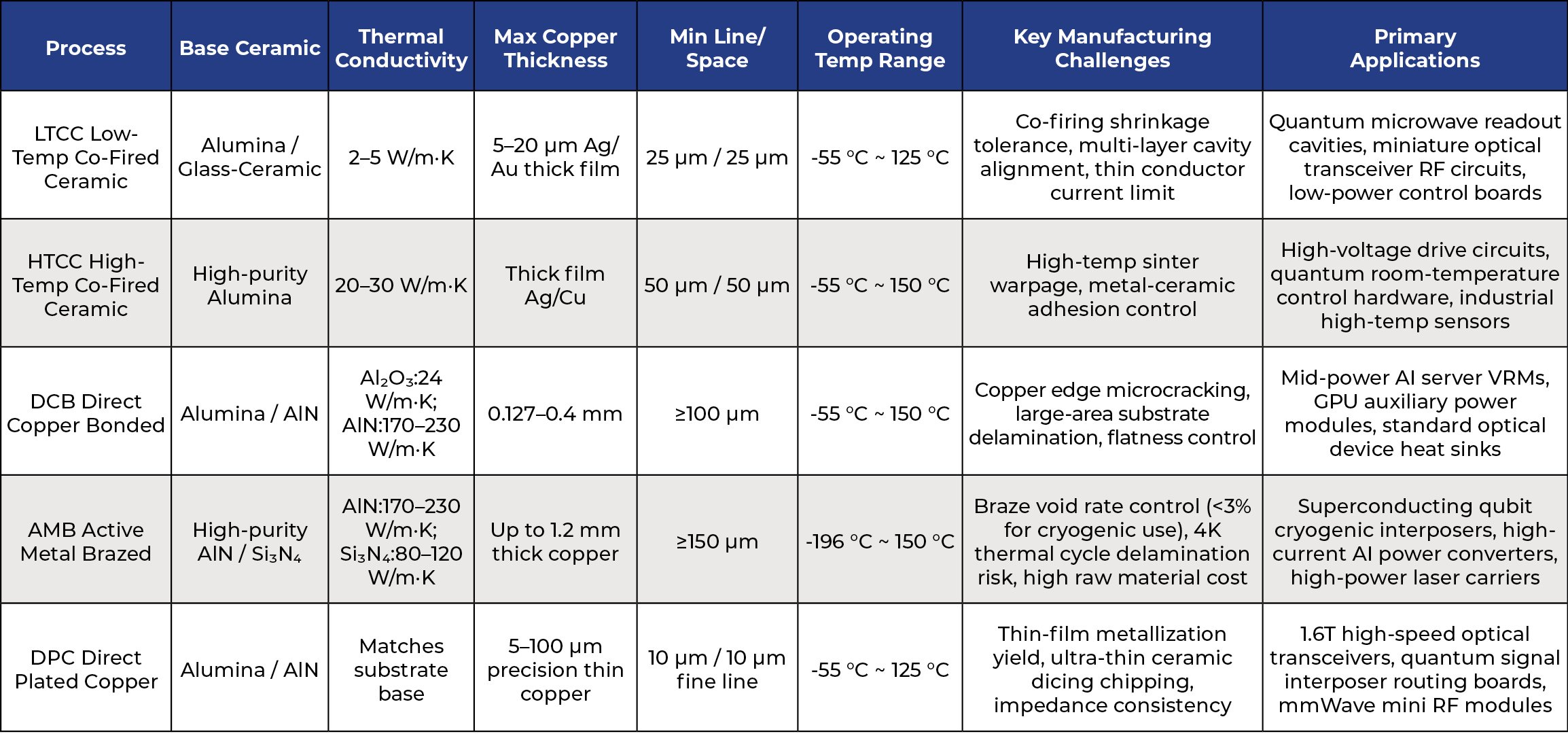
Most articles lump all ceramic boards as “ceramic PCBs”, ignoring fundamental manufacturing limits that determine yield, cost and application compatibility. Below is a clear comparison of process boundaries, minimum feature sizes, factory production bottlenecks and target use cases:
Need Support With a Ceramic PCB Project?
Explore PICA’s ceramic PCB capabilities for high-heat, high-frequency, and high-reliability applications. Our team can help evaluate material options, manufacturability, and production requirements for your next design.
Supplementary Material & Surface Finish Guidance
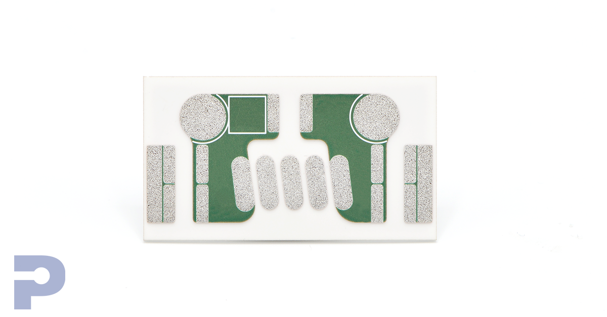
Available platings: Ni, Ag, Ni+Au. Selection rules for production:
• Cryogenic quantum hardware: Ni/Au finish to avoid silver oxidation and microwave signal loss
• High-current power modules: Thick Ni barrier layer to prevent copper migration
• LTCC RF cavities: Silver thick film for low-frequency signal transmission
Chemical compatibility note: Substrate stack-up (ceramic + copper + finish + assembly adhesive) must be validated against cleaning solvents; improper material matching causes peeling or surface corrosion during mass production. PICA’s engineering team conducts pre-production material durability reviews to eliminate post-assembly failure risks.
3. Ceramic Substrate Implementation in Quantum Computing (Cryogenic-Specific Design & Production Standards)
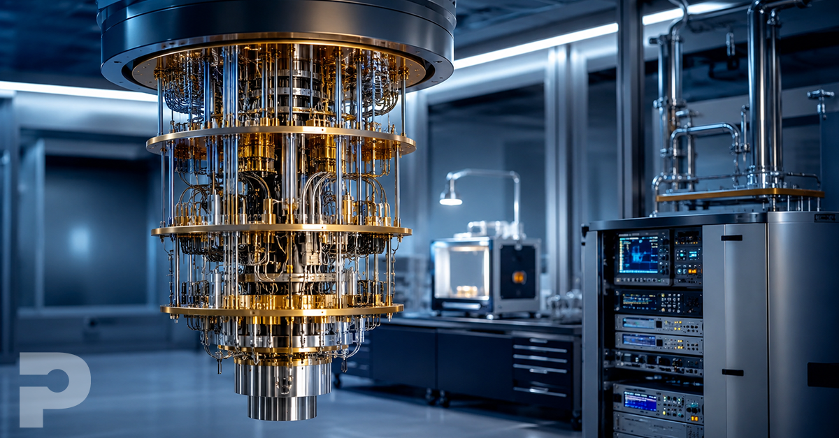
Superconducting quantum processors operate at 4K liquid helium temperatures. Even minor substrate warpage, thermal expansion mismatch or microwave insertion loss degrades qubit coherence. Ceramic substrates function as cryogenic interposers, microwave routing carriers, control circuit platforms and packaging support structures—with strict process requirements that factories must follow during fabrication.
3.1 Thermal Stability for 4K Cryogenic Environments
Ordinary alumina DCB cannot withstand repeated cryogenic cycling due to mismatched CTE between copper and ceramic.
• Recommended solution: AMB AlN substrates with 2.6 ppm/°C low-CTE tuning
• Factory mandatory inspection: 100% X-ray void detection for braze layers; full -196 °C ↔ 25 °C thermal cycle qualification before delivery
• Design restriction: Avoid multi-material bonding stacks with dissimilar CTE values; all adhesive layers must be cryogenically rated
3.2 Low-Loss Signal Integrity for Qubit Control & Readout
Qubit manipulation relies on high-frequency microwave pulses; impedance mismatch or dielectric loss introduces noise that distorts readout data.
• Miniature multi-layer RF cavities: LTCC co-fired structures integrate filters to reduce external component count
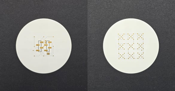
• Fine-line high-speed signal interposers: DPC 10 μm line/space maintains tight impedance tolerance across cryogenic temperature swings
• Manufacturing limit reminder: LTCC shrinkage offset must be compensated in PCB Gerber files; DPC thin copper layers require laser direct imaging to avoid impedance variation
Common Quantum Hardware Design & Production Fail Points
• Selecting alumina DCB for cryogenic use → copper-ceramic delamination after thermal cycling
• Over-thick metal layers on LTCC boards → excessive heat load inside dilution refrigerators
• Skipping X-ray void inspection on AMB substrates → localized hotspots and qubit signal interference
4. Ceramic Substrates for AI & High-Performance Data Centers
Data center hardware faces room-temperature high-power density challenges instead of cryogenic conditions: AI GPUs, voltage regulation modules, and 800G/1.6T optical transceivers generate concentrated heat at 24/7 continuous load. Ceramic substrates resolve thermal bottlenecks while stabilizing high-speed signal transmission.
4.1 AI Server High-Power Electronics & VRMs
High-performance GPU clusters require high-current power conversion with effective board-level heat dissipation:
• Mid-density power modules: Alumina DCB (0.127–0.3 mm copper thickness) balances cost and thermal performance
• Ultra-high-power 3kW+ accelerator units: AMB AlN with 0.8–1.2 mm thick copper for extreme current carrying capacity
• Factory production control: Strict substrate flatness specs to prevent assembly solder joint cracking; thermal resistance sampling testing for every batch
• Design pitfall: Excessively thick copper layouts create uneven heat distribution and substrate warpage under full load
4.2 High-Speed Optical Transceivers (800G / 1.6T)
High-bandwidth data interconnections demand miniaturized, low-loss substrates for optoelectronic integration:
• Ultra-fine signal routing: DPC thin-film copper achieves 10 μm line/space for consistent high-frequency impedance
• Optical device heat dissipation: Thin AlN DCB carriers eliminate thermal crosstalk between adjacent channels
• Fabrication constraint: Ultra-thin ceramic base plates (<0.25 mm) require laser dicing to prevent edge chipping and low assembly yield
5. Material Selection as a Core Competitive Advantage for Advanced Computing
Chip performance is no longer the sole bottleneck for quantum and data center hardware. Packaging, interconnection, thermal management and substrate dielectric properties directly determine long-term system uptime and scalability.
• For quantum systems: AMB AlN delivers cryogenic dimensional stability; LTCC/DPC enable compact low-noise microwave routing
• For AI data centers: DCB/AMB handle high-power thermal loads; DPC supports high-speed optical module miniaturization
Standard FR-4 remains cost-effective for low-power, low-frequency consumer hardware, but ceramic substrates become non-negotiable under extreme thermal, frequency or cryogenic operating conditions.
6. End-to-End Ceramic Substrate Engineering Support from PICA (Actionable, Factory-Oriented)
PICA’s engineering team aligns with both hardware designers and ceramic PCB manufacturers to resolve DFM, material and production risks early in the design cycle, with standardized deliverables:
• Application requirement decomposition: Clarify operating temperature (4K cryo / room temp), power load, signal frequency, production volume and reliability standards
• Material & process matching: Generate LTCC/HTCC/DCB/AMB/DPC shortlist with quantified cost and yield tradeoffs
• DFM manufacturability review: Flag factory processing limits (minimum line width, copper thickness, cavity depth, dicing tolerance) to avoid redesign iterations
• Mass production process normalization: Output production specifications for ceramic manufacturers to stabilize batch yield
We support projects covering high-heat, high-frequency, high-voltage, cryogenic and harsh-environment ceramic substrate requirements.
7. Partner With PICA for Ceramic PCB Design & Manufacturing Optimization
Ceramic substrates are not universal drop-in replacements for FR-4; improper material or process selection leads to low yield, system performance degradation and increased production costs.
If your design requires superior thermal dissipation, consistent high-frequency signal performance, or stable operation under extreme temperature cycling, PICA’s cross-functional engineering team can conduct early-stage material reviews, DFM feasibility audits and coordinate process alignment with your ceramic board manufacturing partners to cut development cycles and reduce mass production risks.
Conclusion
Ceramic substrates can help advanced computing hardware manage heat, high-frequency signals, and demanding operating conditions that traditional FR-4 boards may not handle well. Choosing the right material and process early helps reduce design risk, improve reliability, and support a smoother path to production. PICA can help evaluate ceramic substrate materials, manufacturability, and production considerations early in the design process.