 English

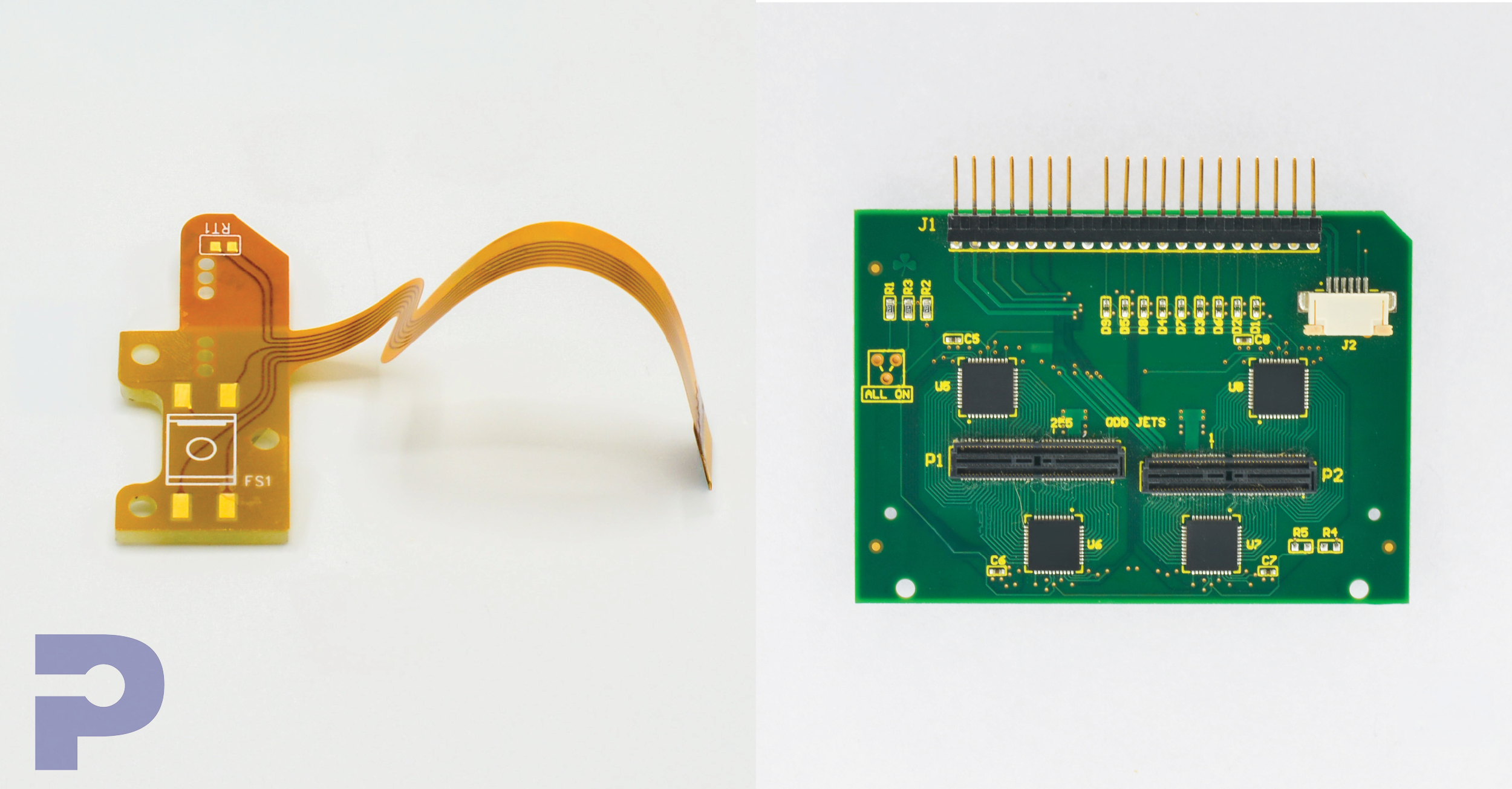
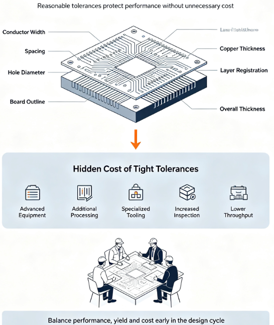
Printed circuit board tolerances define how much a manufactured feature may vary from its specified dimensions. Every PCB requires tolerances for features such as conductor width, spacing, hole diameter, board outline, copper thickness, layer registration, and overall thickness. However, specifying tighter tolerances than the application requires can significantly increase the cost of both flexible and rigid printed circuit boards.
Tight tolerances do not simply require a PCB manufacturer to be more careful. They may require more advanced equipment, additional processing, tighter material controls, specialized tooling, increased inspection, and lower manufacturing throughput. They can also reduce the number of acceptable circuits produced from each manufacturing panel.
Understanding where tolerances affect cost can help engineering and sourcing teams establish requirements that protect product performance without adding unnecessary manufacturing complexity.
What Is a PCB Tolerance?
A PCB drawing typically contains a nominal dimension followed by an acceptable range of variation. For example, a finished hole may be specified as 0.250 mm ±0.075 mm. Any finished hole within that range would meet the requirement.
PCB tolerances may apply to:
• Trace width and conductor spacing
• Drilled and finished hole diameters
• Annular rings
• Board or flex-circuit outlines
• Slot and cutout dimensions
• Copper and plating thickness
• Dielectric thickness
• Overall circuit thickness
• Coverlay and solder mask registration
• Stiffener placement
• Controlled impedance
• Component and connector locations
Standard manufacturing tolerances are based on the expected variation of the materials, equipment, and processes used to build the circuit. When a requirement falls outside those standard capabilities, the manufacturer must introduce additional controls to maintain it.
Why Do Tighter PCB Tolerances Cost More?
Tighter tolerances can reduce manufacturing yield
Manufacturing yield is the percentage of circuits that pass inspection and can be shipped. It is one of the most important factors influencing PCB cost.
Consider a circuit outline that can normally vary by ±0.20 mm. If the drawing reduces that allowance to ±0.05 mm, boards that would have met the manufacturer’s standard tolerance may now be rejected. The PCB manufacturer must account for the expected scrap when preparing the quotation.
This issue becomes more significant when multiple tightly controlled features are placed on the same circuit. A board may meet nine requirements but fail one unusually restrictive dimension. Because the entire circuit may then be rejected, the cost of every acceptable board increases.
Additional inspection may be required
Standard PCB features are inspected using automated optical inspection, electrical testing, dimensional measurements, microsection analysis, and other process controls. Tight tolerances can require more frequent measurements, specialized metrology equipment, additional test coupons, or 100% inspection of a particular feature.
Inspection does not add functionality to the PCB, but it provides evidence that the finished circuit meets the requirement. The associated labor, equipment time, documentation, and potential rework become part of the manufacturing cost.
Ready to Optimize Your PCB Design?
Avoid unnecessary costs by reviewing tolerances early in the design process. Explore PICA’s PCB solutions and work with our team to balance precision, manufacturability, reliability, and cost.
Production equipment may need to operate more slowly
Processes such as imaging, drilling, routing, laser cutting, lamination, plating, and registration have natural variations. Maintaining a narrow tolerance may require slower machine settings, more frequent tool changes, tighter environmental controls, or additional calibration.
A smaller drilled hole, for example, may appear to be a minor design change. In practice, it can require different drill tools, reduced stack heights, more frequent drill-bit replacement, and tighter plating control.
Specialized tooling or processes may be necessary
Standard routing, drilling, imaging, and punching methods are generally the most economical because they can be used efficiently across many designs. Tight dimensional requirements may instead require laser processing, hard tooling, precision registration systems, sequential processing, or custom fixtures.
The cost difference can be especially noticeable during prototype and low-volume production, where tooling expenses are spread across relatively few circuits.
Key cost effect: The tighter the allowable variation, the smaller the manufacturer’s process window. A smaller process window typically means more control, more inspection, and a higher risk of scrap.
Which Tolerances Commonly Increase Rigid PCB Costs?
Fine conductor width and spacing
As traces and spaces become smaller, controlling the imaging and etching process becomes more difficult. Small variations in copper thickness, photoresist, exposure, and etching can affect the finished conductor dimensions. Fine features may require advanced imaging equipment, modified copper weights, tighter process controls, and increased inspection. They can also reduce manufacturing yield, particularly when fine features cover a large portion of the panel.
Small holes and annular rings
Small drilled holes require precise drilling and plating. When a small hole is combined with a narrow annular ring, any variation in drill position or layer registration can reduce the remaining copper around the hole. Increasing the pad size or allowing a larger annular ring generally improves manufacturability. Conversely, reducing the annular ring may require tighter registration, more advanced drilling, and additional inspection.
Overall board thickness
Rigid PCB thickness is influenced by the copper, laminate, and prepreg materials used in the stackup, along with the behavior of the materials during lamination. A highly restrictive overall-thickness tolerance may require custom material selection, additional measurements, and tighter lamination controls. Thickness becomes especially important for edge connectors, press-fit components, mechanical enclosures, and assemblies using recessed or cavity structures.
Board outlines, slots, and cutouts
Mechanical features frequently interface with enclosures, connectors, fasteners, or other parts. Requiring extremely accurate routing or slot dimensions may require smaller routing tools, slower feed rates, multiple finishing passes, or specialized tooling.
Why Are Tolerances Especially Important in Flex PCBs?
Flexible circuits introduce additional dimensional movement because the materials are thin and flexible. Polyimide films, adhesives, copper foils, and coverlay materials can expand, contract, stretch, or shift during imaging, lamination, handling, and thermal processing.
A dimensional tolerance that is routine on a rigid PCB may therefore be more difficult to maintain on a flexible circuit.
Material movement affects feature registration
Flex materials can change dimensions as they move through the manufacturing process. Manufacturers compensate for expected material movement when preparing imaging and tooling, but extremely tight feature-to-feature tolerances may still require additional process controls. Registration requirements commonly affect coverlay openings to copper pads, stiffener placement, connector finger locations, hole-to-outline dimensions, component locations, and flex-to-rigid transition areas.
Stiffener placement can affect connector alignment
Stiffeners are frequently added beneath connectors, soldered components, or contact fingers. If the stiffener must align very precisely with the circuit outline, holes, or contact area, the manufacturer may need dedicated alignment fixtures or precision placement equipment. The required tolerance should reflect how the stiffener functions. A connector-contact area may justify close control, while a stiffener that only provides general mechanical support may allow a wider placement tolerance.
Outline tolerances depend on the singulation method
Flexible circuits may be separated from a production panel using steel-rule dies, hard tooling, laser cutting, routing, or other methods. Each process offers a different combination of accuracy, tooling cost, edge quality, and production speed. A complex outline with tight dimensional requirements may require laser processing or precision hard tooling rather than a more economical standard method.
How Can Designers Control PCB Tolerance Costs?
The most effective approach is to apply tight tolerances only where they support a genuine electrical, mechanical, assembly, or reliability requirement.
• Identify dimensions that are critical to function.
• Use the manufacturer’s standard tolerances for noncritical features.
• Avoid applying a restrictive general tolerance to the entire drawing.
• Dimension critical features from a common datum.
• Consider material movement when locating features on flex circuits.
• Allow adequate annular rings around drilled holes.
• Review connector, enclosure, and component requirements carefully.
• Discuss unusual tolerances with the PCB manufacturer before design release.
It is also helpful to distinguish between a preferred target and an absolute acceptance requirement. When every drawing dimension receives the same tight tolerance, the manufacturer must quote and inspect the entire circuit as though every feature were equally important.

Balance Precision With Manufacturability
PCB tolerances protect fit, function, electrical performance, and reliability, but tighter is not automatically better. Every reduced tolerance creates a potential trade-off involving equipment capability, processing time, inspection, yield, tooling, and material behavior.
The goal should be to establish tolerances that are tight enough to support the product without exceeding what the application actually needs. Early design-for-manufacturability discussions can help engineering teams identify critical dimensions, adjust noncritical requirements, and avoid tolerance-related cost increases before production begins.
Need help reviewing tolerance requirements? PICA Manufacturing Solutions works with customers to evaluate flex and rigid PCB drawings, stackups, mechanical interfaces, and critical feature requirements. Contact our team to discuss how tolerance decisions may affect the manufacturability, reliability, and cost of your next PCB design.
References
• IPC, PCBA Checklist and producibility guidance
• Würth Elektronik, Printed Circuit Board Basics
• IPC technical resource on PCB thickness tolerance and cavity design