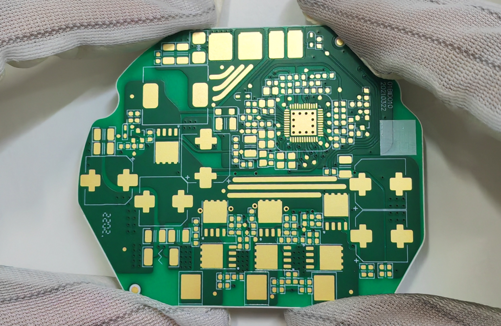
Ceramic substrate PCBs (Printed Circuit Boards) represent a significant advancement in circuit board technology, especially when compared to traditional FR4 boards commonly used in electronics. These ceramic-based boards are gaining popularity due to their superior heat management, stability, and reliability. Ceramic PCBs are increasingly employed in high-demand sectors such as electric vehicles, medical devices, aerospace, rail transit, and power transmission networks.
- Types of Ceramic Substrates:
- AL2O3/ZTA series: This type is extensively used because it provides a good balance of key properties needed for many electronic applications.
- ALN (Aluminum Nitride): Known for its exceptional thermal conductivity, ALN, a common choice for Ceramic PCBs, is ideal for applications where efficient heat transfer is critical.
- Si3N4 (Silicon Nitride: It is remarkable for its low rate of expansion and contraction with temperature changes, a crucial feature for Ceramic PCBs, known as the Coefficient of Thermal Expansion (CTE). This feature is crucial for maintaining structural integrity and consistent performance in varied thermal environments. - Fabrication Processes:
- 2-1 Direct Bond Copper (DBC): DBC involves the direct bonding of copper to a ceramic substrate (typically alumina or aluminum nitride) without any additional layers or adhesives. The process usually occurs in a high-temperature and high-pressure environment. The DBC process is cost-effective and relatively simple in terms of manufacturing, making it widely used in Ceramic PCBs. However, its thermal conductivity is lower than other methods, and it’s less capable of handling extreme temperature changes. It’s widely used in applications like power drives, electric vehicles, and various medical devices, where the benefits of ceramic substrates are desired but extreme conditions are not a factor.
- 2-2 Active Metal Brazing (AMB): AMB involves a brazing technique where an active metal (like titanium) is used in the brazing alloy to facilitate the bonding of copper (or other metals) to the ceramic substrate (commonly alumina, sapphire, or silicon nitride). These materials are exceptional for thermal management and reliability, making AMB ideal for high-stress applications involving high voltages or extreme thermal conditions, such as in advanced medical equipment, aerospace technologies, and high-speed rail systems. Although AMB is more complex and costly compared to DBC, the performance benefits it offers are substantial, particularly in high-tech industries. - Manufacturing Process of Ceramic Substrate PCBs: The manufacturing process involves several intricate steps. It begins with the ceramic substrate, followed by laser drilling to create precise holes. Then, metal layers are applied through a process called magnetron sputtering. The board is then coated with a dry film, exposed to develop the circuit layout, and undergoes various finishing processes including etching and solder masking. Each of these steps is critical to ensure that the PCB can effectively conduct electrical signals and withstand the operational environment it’s designed for.
PICA delivers precision-engineered ceramic circuit boards with exceptional thermal management and reliability for demanding environments. Optimize your design with cutting-edge ceramic PCB solutions
In essence, ceramic substrate PCBs are at the forefront of electronic circuit board technology, offering exceptional benefits in heat management, structural stability, and overall reliability. Their versatility and high performance make Ceramic PCBs a preferred choice in advanced electronic applications, where traditional materials might not meet the demanding requirements. As technology continues to evolve, the use of ceramic substrate PCBs is likely to expand, paving the way for more innovative and efficient electronic solutions.
