 English

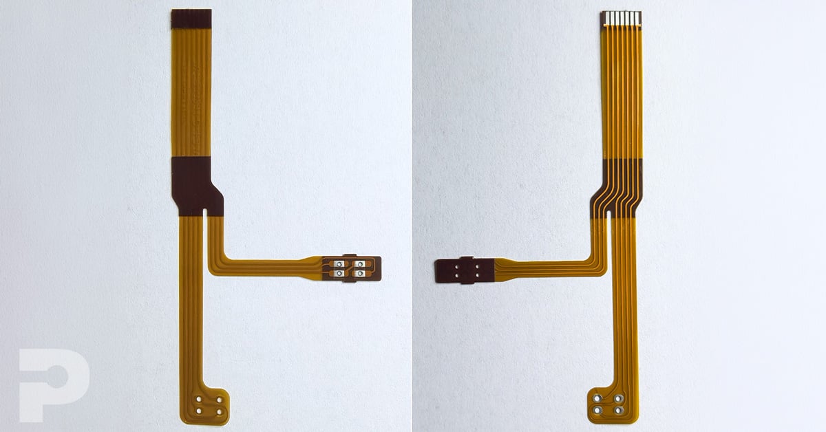
When a design requires electrical contact from both sides of a flex circuit, two copper layers may not be necessary. A double-access flex circuit exposes selected areas of a single copper layer through openings in the surrounding insulation. The construction affects contact geometry, alignment tolerances, and support for exposed conductors.
What double access means
A conventional double-sided flex circuit has two copper layers. A double-access circuit has one conductive layer that can be contacted from either side at designated locations. Those locations do not have to be identical on both sides.
Two manufacturing approaches are pre-windowed coverlay construction and selective polyimide etching. Availability and achievable features depend on the manufacturer’s materials, equipment, and process capabilities.
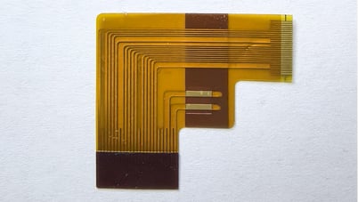
Figure 1. Openings in the insulating coverlay expose selected contact areas while the surrounding conductors remain protected
Pre windowed coverlay construction
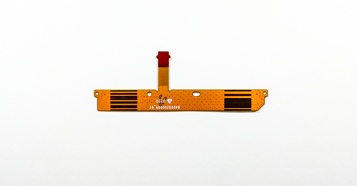
Coverlay is an insulating film, typically polyimide with an adhesive layer, used to protect flex circuit conductors. In this approach, access openings are cut into the adhesive-backed film before copper foil is laminated to it. The copper is then imaged and etched to form the circuit pattern. A second coverlay protects the other side, with openings where electrical access is required.
The opening pattern must align with the copper features through lamination and circuit fabrication. Adhesive flow also needs to be controlled so it does not reduce the usable contact area.
Designing the access openings
Start by identifying which contacts must be accessible from each side and the minimum exposed area needed for the connection. An opening that looks adequate in a drawing may leave too little usable contact area once alignment variation and adhesive flow are considered.
Review these details with the manufacturer before releasing the design:
- Opening dimensions and position relative to the copper contact.
- Alignment tolerances between the openings and the circuit pattern.
- Clearance for adhesive flow and insulation overlap around exposed features.
- Support for copper exposed through overlapping openings on both sides.
Where the same feature is exposed from both sides, the openings may need to differ in size to suit the fabrication process. Use the manufacturer’s design rules rather than assuming that a single opening size or tolerance applies to every construction.
Selective polyimide etching
Another approach begins with a copper-clad polyimide laminate. Selected areas of the polyimide are chemically removed to expose the copper. An etch-resistant mask defines the areas to be opened; the sequence relative to copper patterning depends on the process.
Selective etching can accommodate openings that are difficult to produce mechanically, but it does not guarantee smaller features or tighter alignment. Material compatibility, mask registration, etching chemistry, and process control determine what is practical. Incomplete removal can leave insulation over a contact, while excessive etching can reduce support around the exposed conductor.
Treat this as a process option to discuss with the manufacturer. Confirm that it is available for the intended material stackup and production volume.
Potential manufacturing problems
Need Help With Your Flex Circuit Design?
Work with PICA Manufacturing Solutions to evaluate materials, construction, and assembly requirements. Our team can help you develop a flex circuit that meets your application’s performance and manufacturing needs.
When double access becomes flying leads
Access from both sides does not automatically mean a circuit has flying leads. Flying leads, also called free-standing leads, are conductor sections that span an opening or extend beyond the insulating support.
Depending on the construction, either manufacturing approach can create these unsupported sections. They offer a way to connect directly to another component or terminal, but require attention to conductor width, copper thickness, unsupported length, and assembly forces.
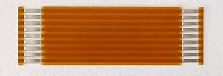
Figure 2. Unsupported conductor sections span the gaps between the main insulated circuit and the narrow outer support strips. These flying leads need protection during handling and assembly.
Choosing a practical construction
The useful question is whether a process can consistently produce the required contact geometry and support the intended assembly method at the planned volume. A smaller opening is valuable only if it leaves enough usable contact area and can be manufactured reliably.
Bring the manufacturer a drawing that identifies access from each side, required contact areas, opening dimensions, material stackup, and any unsupported conductor sections. Include the intended assembly method, expected mechanical loading, and anticipated production volume. Ask for achievable tolerances and recommended design changes before fixing the geometry.
At PICA Manufacturing Solutions, we work with OEM engineers early in development to evaluate these requirements and identify a practical flex circuit construction. Contact our team to review your double-access flex design before releasing it for production.