X-ray inspection exposes hidden defects in solder joints, BGAs, vias, and internal connections that are invisible with visual or AOI inspection. By catching voids, shorts, opens, and bridges early, X-ray helps prevent expensive rework, improve yields, and ensure long-term reliability.
Electrical reliability is often determined by what you cannot see. In this article, we explain what X-ray inspection reveals, when to use it, and how it helps engineers troubleshoot failure risks before assembly leaves the line.
What X-Ray Inspection Detects in PCB Assemblies
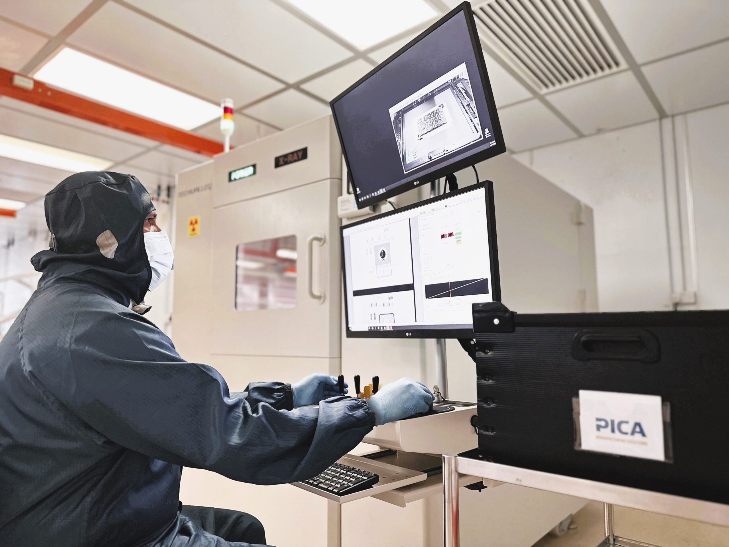
In the realm of flexible printed circuit assembly (FPCA) and printed circuit board assembly (PCBA), X-ray inspection plays a crucial role in ensuring product quality and meeting stringent requirements. This is particularly vital when incorporating surface mount components such as ball grid array (BGA), land grid array (LPA), chip scale package (CSP), and MEMS devices like microphones for the mobile market. Recognizing this, Pica Manufacturing Solutions (PMS) has strategically upgraded its X-ray inspection capabilities, particularly at its Malaysian division, PMS Malaysia (PMSM).
Why X-Ray Is Critical for BGA, CSP, and MEMS Devices
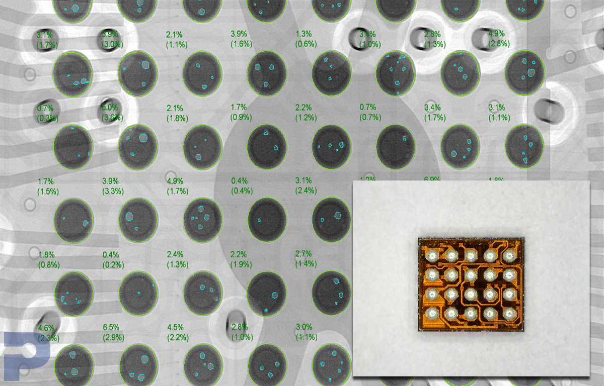
The challenge in manufacturing products using BGA, LGA, CSP, and MEMS devices lies in the hidden solder pads located on the package substrate. Traditional inspection methods like optical, ultrasonic, and thermal imaging often miss these hidden solder joints, leading to potential quality issues. The X-ray inspection system, therefore, becomes essential in PCBA/FPCA processes for its ability to conduct non-destructive testing of internal PCB/FPC structures. It excels in identifying solderability issues such as voids and solder bridge detection.
Essential features of the X-ray inspection system include:
- Void automatic measurement and analysis.
- Geometrical measurements including distance, length, angle, and through-hole measurements.
- Wire length measurement.
- 3D CT scanning.
- Automated inspection routines for repeated inspection of the same products.
Hidden solder defects don’t need to be guesswork.
Our on-site X-ray inspection service helps engineers verify reliability, troubleshoot yield issues, and prevent downstream failures.
Common Defects X-Ray Reveals That Other Tests Miss
Voids analysis, a key feature of the X-ray inspection system, is particularly crucial for BGA, LPA, CSP, and MEMS devices. Voids, or air pockets within solder joints, significantly impact the reliability and functionality of products. For instance, excessive voids in MEMS microphone devices can lead to audio issues. The X-ray inspection system is instrumental in detecting void rates in solder joints, driving process improvements to minimize these defects.
X-Ray Capabilities at PICA Manufacturing Solutions
PMSM’s implementation of the X-ray inspection system has enhanced several key capabilities beyond void analysis:
- Wire bond inspection for verifying wire bond quality.
- Internal layer inspection of FPC/PCB, including:
• Continuity verification of copper traces.
• Internal structure inspection of surface-mount devices (SMD) to ensure correct component mounting during the SMT process.
When to Use X-Ray in Your Build Process
In conclusion, the X-ray inspection system is an indispensable tool for elevating in-house inspection standards at PMSM. It significantly improves quality control in SMT processes, aids in failure analysis of incoming bareflex and SMD components and enhances overall productivity.
Need Help Interpreting Inspection Results?
Have assembly reliability concerns? Our engineering team can walk through your X-ray inspection requirements and help troubleshoot yield issues.
