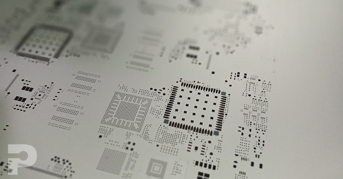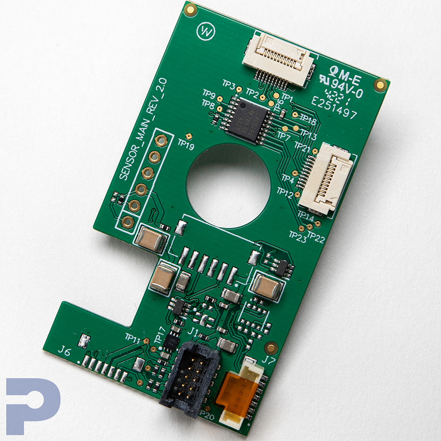
Stencil design plays a critical role in ensuring the quality and reliability of printed circuit boards (PCBs). A well-designed stencil enables precise solder paste deposition, ensuring strong solder joints and high manufacturing yields. With over 30 years of experience and facilities in Derry, NH, and Kuala Lumpur, Malaysia, PICA has a proven record of excellence in designing stencils for a wide range of applications. Below are the key factors to consider when designing a stencil for effective performance and durability.
Critical Characteristics of the Stencil
1. Chip Component Opening Separation Proper separation between openings for chip components is essential to prevent solder bridging. Adequate spacing ensures clean and precise paste deposits, reducing defects during the reflow process.
2. A stencil opening larger than the PCB copper pad may cause solder bridging, especially if the paste is deposited over an uneven surface, such as via holes. Conversely, an opening smaller than the PCB copper pad may result in insufficient solder deposition, leading to weak solder joints.
Recommended stencil opening sizes:
• Chip/passive components: 1:1 opening (100% of the copper pad size)
• Integrated Circuits (ICs): 60–80% of the copper pad size
• Fine-pitch lead components: 60% of the copper pad size
3. High Grab Factor A stencil with a high grab factor ensures better adhesion of solder paste to component pads, improving placement accuracy and overall assembly quality. The grab factor reflects the effectiveness of solder paste adhering to the stencil and transferring cleanly onto the PCB pads. This factor is influenced by stencil material, aperture finish, and solder paste properties.
Recommended design considerations:
• Aspect ratio (aperture width to stencil thickness) should be >1.5
• Area ratio (aperture opening surface area to wall surface area) should be >0.66
4. Stencil Thickness Selection Stencil thickness must balance the solder volume requirements for large and small components.
• Thinner stencils (0.1–0.12 mm): Best for fine-pitch components
• Thicker stencils (0.15–0.2 mm): Suitable for larger components requiring more solder
5. For PCBs that contain both fine-pitch and larger components, step stencils are recommended. Step stencils offer varying thicknesses across different areas of the stencil to optimize solder volume distribution. However, these stencils come at a higher fabrication cost compared to standard stencils.
6. Solder Volume for Various Components A well-designed stencil must account for different solder volume requirements:
• Sufficient solder volume for larger components to ensure proper wetting
• Controlled solder deposition on smaller pads to prevent bridging or tombstoning
Want to learn more about Pica’s capabilities in PCB design?
Explore our high-quality, custom printed circuit boards designed to fit your unique needs. Whether it’s for consumer electronics, automotive, or medical devices, we’ve got you covered with precision engineering and reliable performance.
Alignment and Material Considerations
1. Fiducial Marks as Alignment Features Fiducial marks are critical for ensuring accurate alignment between the PCB and the stencil. A minimum of three fiducial marks per PCB panel is recommended for optimal alignment and repeatability.
2. Stencil Material and Fabrication Methods Stencils are typically made from stainless steel or nickel due to their durability and precision. Aperture openings are created using:
• Laser cutting (provides superior accuracy for intricate designs)
• Chemical etching (less precise, suitable for basic designs)
• Electroforming (offers excellent precision for high-density applications)
3. Electro-Polishing & Micro-Plating Electro-polishing smoothens aperture walls, improving solder paste release and reducing defects. A micro-plating process can further enhance release properties, leading to higher manufacturing yields.
4. Durability & Service Life Stainless steel stencils are known for their longevity, particularly when properly maintained. Electroformed nickel stencils offer additional strength and are ideal for high-volume production and densely populated PCBs.
Compensation for Polyimide Sub-Panel Shrinkage
1. Polyimide sub-panels may shrink during manufacturing. To compensate for this, stencil openings must be adjusted through dimensional analysis to ensure alignment with IPC-610 standards for solder joint geometry.
Design Guidelines
1. Smaller Aperture Size Stencil openings should be slightly smaller than the solder pad to reduce off-pad paste deposition. This approach minimizes the risk of solder bridging and enhances joint reliability.
2. IPC-610 Compliance Designing stencils in compliance with IPC-610 standards ensures solder joint quality, aligning with industry best practices for geometry and reliability.
3. Stencil Opening Design Rules
Round Stencil Openings:
• Aperture opening surface area to hole wall surface area should be ≥ 0.66
Rectangular Stencil Openings:
• Width (W) and length (L) of the stencil opening, when divided by the stencil thickness (T), should be ≥ 1.5:
(W / T ≥ 1.5) and (L / T ≥ 1.5)
• The area of the aperture opening (L × W) divided by the surface area of the aperture side walls should be ≥ 0.66
4. Stencil Opening Shapes for Passive Components Solder balls commonly occur when excessive solder volume is used on passive components. Alternative stencil opening shapes can help mitigate this issue:
• Home-plate shape
• Inverse home-plate shape
• Rounded inverse home-plate shape
By incorporating these critical characteristics and best practices, stencil design can significantly enhance solder paste application, ensuring reliable PCB assembly and robust product performance.
With over 30 years of expertise in stencil design, PICA Manufacturing Solutions is committed to helping customers achieve high-quality Printed Circuit Board (PCB) assemblies. Our experienced team provides tailored solutions to optimize solder paste deposition and ensure manufacturing success. Contact us today to benefit from our industry-leading knowledge and support.
