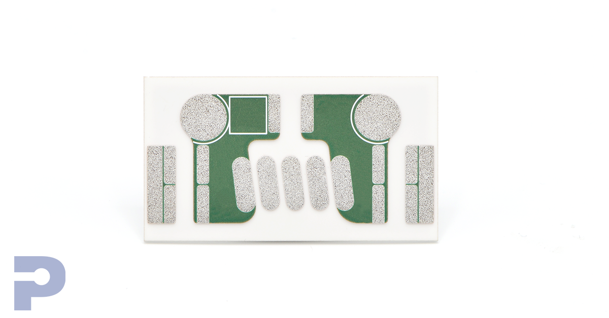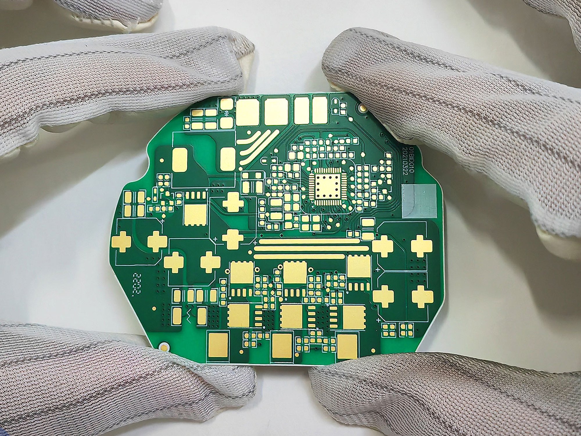
Modern electronics are expected to run hotter, switch faster, and survive harsher environments than ever. Standard FR-4 hits its limits quickly in these scenarios. Ceramic printed circuit boards (PCBs) step in with exceptional thermal conductivity, electrical insulation, and mechanical stability, enabling compact, long-life designs in power, RF/microwave, aerospace/defense, and heavy industrial markets.
PICA Manufacturing Solutions designs and manufactures ceramic PCB assemblies using aluminum oxide (Al₂O₃), aluminum nitride (AlN), and silicon nitride (Si₃N₄).
From prototypes to volume production—and from pure ceramic builds to hybrid ceramic + metal-core or rigid-flex architectures—we align material choice, stackup, and manufacturing to your electrical, thermal, and mechanical goals.
Why Choose Ceramic PCBs?
• Thermal Conductivity: Ceramics pull heat away from junctions far more effectively than FR-4, supporting high-power LEDs, drivers, and power converters.
• Reliability in Harsh Environments: Low coefficients of thermal expansion (CTE) and corrosion resistance help boards stay dimensionally stable under shock, vibration, and extreme temperatures.
• High-Frequency Performance: Low dielectric loss and high breakdown voltage enable efficient RF/microwave and high-voltage designs.
• Compact Design Potential: Dense interconnects, embedded passives, and hybrid configurations reduce footprint while raising performance.
• Long-Term Durability: Excellent resistance to chemical, mechanical, and thermal stress extends field life in critical systems.
Where Ceramic PCBs Shine (Applications & Markets)
Power Electronics & High Voltage
• DC-DC/AC-DC conversion, motor drives, inverters, solid-state relays, battery management, e-mobility power stages.
• Stable isolation and strong heat spreading directly under MOSFETs, IGBTs, GaN/SiC devices.
RF, Microwave & Millimeter-Wave
• Low-loss interconnects for amplifiers, LNAs, PAs, filters, radar front ends, and phased arrays.
• Predictable dielectric properties across temperature for tight phase/noise budgets.
Lighting & Photonics
• High-power LED engines (white/UV/IR), light bars, medical/industrial illumination where thermal resistance and reflectivity matter.
Aerospace, Defense & Harsh Industrial
• Down-hole tools, avionics, radar, actuation systems, high-G environments—where vibration, temperature cycling, and reliability are non-negotiable.
Sensing & Instrumentation
• Pressure/flow/chemical sensors, precision analog, and high-stability timing where CTE and moisture resistance drive stability.
Cryogenic Reliability for Quantum Applications
Ceramic PCBs provide exceptional stability at cryogenic temperatures, making them ideal for quantum computing and superconducting applications. With proven thermal shock resistance from -55 °C to +150 °C and ultra-low CTE values (as low as 2.6 ppm/°C for Si₃N₄), ceramic substrates maintain structural integrity and electrical performance in extreme cold. This ensures reliable operation in dilution refrigerators and cryogenic chambers where conventional PCB materials would fail.
Ceramic Materials—Picking the Right Substrate
• Alumina (Al₂O₃): The workhorse ceramic—excellent electrical insulation (insulation strength 20KV/mm), strong mechanical properties, and good value.
• Aluminum Nitride (AlN): Very high thermal conductivity (>=170 W/(m·K)) with good electrical insulation—ideal for high-power density and fast thermal transients.
• Silicon Nitride (Si₃N₄): Outstanding fracture toughness (Bending Strength 600~700MPa) and thermal shock resistance—favored where mechanical robustness is paramount (e.g., automotive power modules).
Material choice is a system decision: target thermal resistance (junction-to-case/board), voltage standoff, package mechanics, and cycling profile to select the best ceramic for the job.
Ready to explore ceramic PCBs?
Partner with PICA for cooler, more compact, and reliable systems—built to perform in the toughest environments.
Ceramic PCB Stackups & Build Styles
Ceramic is not a single process—several metallization and lamination approaches exist. PICA supports the major families and helps you select the right one.
1) Thick-Film & Thin-Film on Ceramic
• Thick-film (Thick Printing Ceramic Substrate (TPC), e.g., Ag, Ag-Pd, Au pastes; typical thickness 10~20μm) screen-printed and fired on ceramic; robust for power and hybrid circuits.
• Thin-film (Thin Film Ceramic Substrate (TFC), e.g., sputtered TiW/Cu/Au; typical thickness <10μm, most <1μm) for precision RF/microwave lines and tight tolerances -
• Pros: Excellent dimensional stability; configurable conductor/resistor networks; good for hybrids.
• Use cases: RF modules, sensor substrates, precision analog, LED modules, hybrid microelectronics.
2) DBC / AMB (Direct-Bonded Copper / Active-Metal Brazed)
• DBC: Copper directly bonded to ceramic (commonly Al₂O₃, AlN). High thermal conductivity path from device to copper to ceramic.

• Use cases: Power modules, inverters, motor drives, e-mobility traction and charging, solid-state relays.
3) Multilayer Ceramics (HTCC / LTCC)
• HTCC (High-Temp Co-Fired Ceramic): Layers of ceramic tapes with metallization (W/Mo/Mn) co-fired at high temperature (1600 - 1800℃)—durable and hermetic-capable.• LTCC (Low-Temp Co-Fired Ceramic): Co-fires at lower temps (900 - 1000℃) to allow silver/gold conductors and embedded passives (R/L/C) within the stack.
• Pros: True multilayer routing, embedded passives, controlled impedance, miniaturization.
• Use cases: RF front ends, compact sensor modules, high-reliability hybrid packages.
4) Hybrid Ceramic Stacks
• Ceramic + FR-4 or Rigid-Flex: Put hot or RF-critical sections on ceramic; host logic/connectivity on FR-4 or rigid-flex; bridge with flex/FFC.
• Ceramic + Metal-Core (MCPCB): Combine ceramic topography with an underlying metal core when mechanical or mounting constraints favor IMS.
• Pros: Best-of-both-worlds performance without over-engineering the whole assembly.
• Use cases: Mixed power/control boards, RF/power combos, compact modules with challenging thermals.
Manufacturing & DFM Considerations (What to Plan Up Front)
Metallization & Finish
• Select conductor system for your environment and process (e.g., Au thick-film for wire-bonding, Cu for high current).
• Surface finishes: ENIG/ENEPIG on plated copper; Au on thick-film for bond pads and solderability.
Layers & Interconnect
• DBC/AMB: Typically 1-2 copper layers per ceramic tile; routing uses etched copper; through-ceramic vias are not used like FR-4.
• HTCC/LTCC: True multilayer with vias created during tape processing—great for miniaturization and embedded passives.
• Hybrid builds: Plan interface pads and mechanical datum features for clean handoffs to flex/rigid or metal-core.
Thermal Path Engineering
• Place power devices directly over large copper pads tied into the ceramic; use short, wide traces and solid copper pours.
• If coupling to a chassis or cold plate, specify backside flatness and TIM (thermal interface material) choices early.
Mechanical Features
• Define slots, chamfers, and keep-outs during substrate fab—ceramic machining is precise but not an afterthought.
• For high-G or vibration, add mounting features that spread load and avoid stress risers at edges.
Assembly Profiles
• Ceramic substrates change thermal mass and heat flow; tune reflow to ensure wetting on large copper pads without overheating fine features.
• For high power, evaluate press-fit, wire-bond, or clip-bond attachment to manage current and thermal rise.
Test & Reliability
• Specify hipot across dielectric, thermal cycling/soak, and powered thermal tests.
• For RF, include S-parameter targets; for power, define ΔT, RθJB/RθJC goals, and acceptable junction temps.
Bring Ceramic Into Your Next Design—Without Compromise
Whether you’re trying to cool a dense SiC power stage, stabilize a sensitive RF front end, or package a rugged module for aerospace/industrial duty, ceramics provide the physical properties that FR-4 can’t. PICA will help you choose the right substrate and stackup, validate the thermal and electrical model, and build a production-ready assembly that meets your performance and cost targets.
Ready to explore ceramic PCBs?
Share your outlines, thermal/electrical targets, and environment. We’ll propose a ceramic (or hybrid) architecture with lead-time, cost, and reliability options—then take it from proto to production.
