 English

Why Flexible Circuit Design Requires a Different Approach
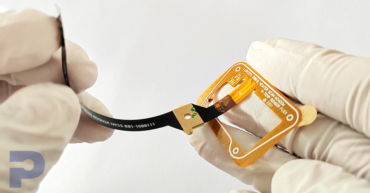
Flexible Printed Circuits (FPCs) are widely used due to their lightweight, flexible, and compact nature, making them ideal for applications requiring bending and folding. However, designing FPCs involves several critical considerations. Engineers should approach FPC design very differently from Printed Circuit Boards (PCBs). PICA Manufacturing Solutions has the expertise to guide engineers in making the right decisions regarding material selection, stack-up design, finishing, and more. Below are common mistakes in FPC design and best practices to address them:
Common Flex PCB Design Mistakes and Best Practices
1. Choosing the Wrong Flex PCB Materials
Mistake: Designers use ED (Electrodeposited) copper instead of RA (Rolled Annealed) copper, leading to cracking during bending. The copper grain direction is often not considered, and final material thicknesses may not meet bending requirements.
Best Practice: Use RA copper for better flexibility, evaluate the necessity of defining the copper grain direction, and ensure the final thickness meets bending needs. Match adhesive thickness in the coverlayer to the copper foil thickness and replace outdated EMI shielding with modern solutions.
2. Using an Unbalanced or Poorly Planned Stack-Up
Mistake: Stack-ups are unsymmetrical, causing warpage. AIR GAPS are often ignored in multi-layer FPCs, and impedance designs may rely on unnecessarily expensive materials.
Best Practice: Ensure symmetrical stack-ups to prevent deformation. Use AIR GAPS between every two layers in multi-layer designs to improve bending reliability. Optimize impedance with cost-effective, flexible materials, and provide requirements to PICA for simulation before finalizing.
3. Overlooking ZIF Connector and Thickness Requirements
Mistake: Stiffeners are mismatched or missing, and material thickness constraints are overlooked.
Best Practice: Use stiffeners like PI, FR-4, or stainless steel for ZIF connectors and evaluate materials carefully to meet strict thickness limits.
4. Submitting Gerber Files with Flex PCB Design Issues
Mistake: IC pads lack proper coverlayer designs, vias are placed too close to flexible edges, and cap openings are too narrow, leading to production issues.
Best Practice: Use gang relieve windows for IC pad designs. Position vias at least 0.6mm away from edges and openings. Design cap openings at least 5mm wide to manage adhesive overflow, though PICA can handle 3mm in extreme cases.
Looking for more Flex PCB design tips? Check out this two part blog called Optimizing Design for Flexible Circuits and request the full white paper download.
5. Specifying an Insufficient Bend Radius
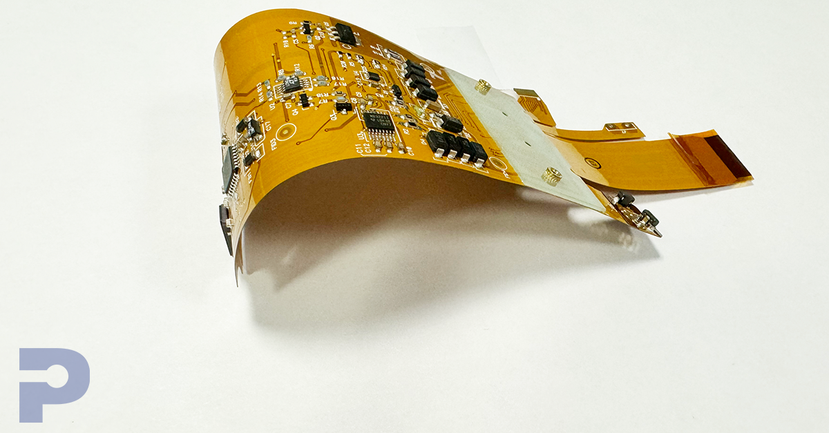
Mistake: Bend radius are specified too small, causing material cracking or failure.
Best Practice: Follow guidelines for minimum bend radius, typically 10x material thickness for dynamic bends and 5x for static bends.
6. Ignoring Thermal Management in High-Stress Areas
Mistake: High-current applications lack proper heat dissipation designs, leading to deformation or delamination.
Best Practice: Use materials with good thermal conductivity and design for even heat dissipation, incorporating thermal vias and heatsinks where necessary.
7. Placing Vias and Connectors in High-Stress Areas
Mistake: Sensitive features like vias and connectors are placed in high-stress bending areas, increasing the risk of failure.
Best Practice: Reinforce stress points with stiffeners and avoid placing sensitive features in bending zones.
8. Failing to Account For Environmental Exposure
Mistake: Designs fail to consider humidity, temperature fluctuations, or chemical exposure, leading to degraded performance.
Best Practice: Use materials that withstand environmental conditions, such as high-temperature adhesives and moisture-resistant coverlays.
9. Skipping Reliability Testing During Prototyping
Mistake: Insufficient testing during prototyping leads to undetected issues that become costly in production.
Best Practice: Perform comprehensive tests for electrical continuity, impedance, and mechanical performance under simulated conditions. For automotive and HDI FPCs, consider 4-wire low-resistance testing for improved reliability.
How PICA Helps Engineers Avoid Flex PCB Design Mistakes
Designing Flexible Printed Circuits (FPCs) requires careful attention to common pitfalls and the application of best practices to avoid them. Proper material selection, thoughtful stack-up design, robust layout rules, and rigorous testing can enhance reliability, reduce costs, and optimize performance. Partnering with experienced manufacturers like PICA Manufacturing Solutions ensures a smooth design process and successful outcomes.