What is Differential Impedance?
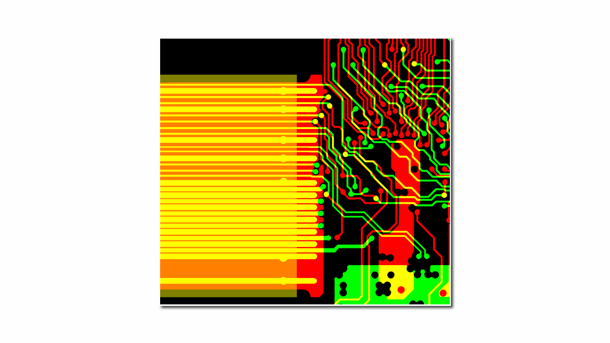
Differential impedance refers to the impedance encountered by a pair of conductors (such as PCB traces) when an equal but opposite signal is driven through them. In high-speed digital circuits, signals are often transmitted using differential pairs, which consist of two closely coupled traces carrying opposite polarity signals. These differential signals help reduce common-mode noise and minimize electromagnetic interference (EMI), making them ideal for high-frequency and high-speed applications.
Differential impedance is a measure of how well these paired conductors can transfer signals without degradation, influenced by factors such as trace geometry, spacing between conductors, the properties of the dielectric material, and the copper thickness. Engineers must carefully calculate and control differential impedance to ensure that signals maintain their integrity as they propagate through the circuit, especially in applications like data centers, telecommunications, automotive systems, and consumer electronics.
Why Differential Impedance Matters in High-Speed PCB Design
In high-speed digital designs, signal integrity is paramount, and any deviation in impedance can lead to significant performance issues. For instance, if the differential impedance is too high or too low compared to the target value, it can cause reflections, signal loss, and increased jitter. The result is often data errors, communication failures, and degraded system performance.
Differential impedance also helps address issues such as:
Crosstalk: When traces are too close, unwanted coupling between signal paths can occur, leading to noise in adjacent signals. Correct impedance control minimizes crosstalk and preserves signal quality.Electromagnetic Interference (EMI): Poor impedance matching can increase radiated emissions, which can interfere with other systems or fail to meet regulatory standards.
Signal Reflections: Impedance mismatches cause signals to reflect back to their source, creating echoes that distort the original signal and degrade overall transmission quality.
PICA ensures accurate signal integrity and consistent electrical performance with expert impedance-controlled PCB manufacturing. Optimize your design with precision engineering
Key Considerations for Engineers in Differential Impedance Management
Several factors play a role in achieving the correct differential impedance in a PCB design. Engineers must take into account:
-
Trace Width and Spacing: The width of the traces and the gap between them directly affect the impedance. Tight tolerances must be maintained to ensure that the impedance stays within the specified range.
-
Dielectric Constant (Dk): The dielectric material between the traces has a significant impact on impedance. Materials with different dielectric constants alter the propagation speed of the signal, affecting the impedance values.
-
Copper Thickness: Thicker copper can reduce the impedance, while thinner copper increases it. Consistent control over copper thickness during manufacturing is vital for impedance control.
-
Stackup Design: The positioning of the differential pairs relative to the ground plane and other layers in the PCB stackup influences the impedance. Stripline configurations, for example, provide better shielding but require precise calculations to maintain desired impedance values.
The Role of Differential Impedance in Flex Circuits
Flex circuits, due to their flexible nature and the use of unique materials, present additional challenges in maintaining controlled impedance. Variations in the substrate's flexibility and the changing environment around the traces can affect impedance consistency. Special design and testing processes are required to account for these variables, ensuring that high-frequency signals are transmitted with minimal loss.
How PICA Manufacturing Solutions Can Help
At PICA Manufacturing Solutions, we understand the complexity of designing for differential impedance, whether in rigid or flex circuits. Our team employs cutting-edge simulation tools and years of expertise to calculate and optimize impedance across all design stages. From material selection to advanced manufacturing techniques, we ensure that your PCB meets the stringent requirements of high-speed digital applications.
Managing differential impedance is non-negotiable for engineers working on high-speed digital communication projects. By addressing factors such as trace geometry, dielectric materials, and copper thickness, engineers can ensure reliable and efficient data transmission. At PICA Manufacturing Solutions, we have the tools, experience, and dedication to help you achieve precise impedance control, optimizing your PCB designs for superior signal integrity. Whether you're designing for telecommunications, automotive, or any other high-frequency application, let us guide you through the complexities of differential impedance to deliver the best possible outcomes.
Reach out to PICA Manufacturing Solutions today and take your PCB designs to the next level.
