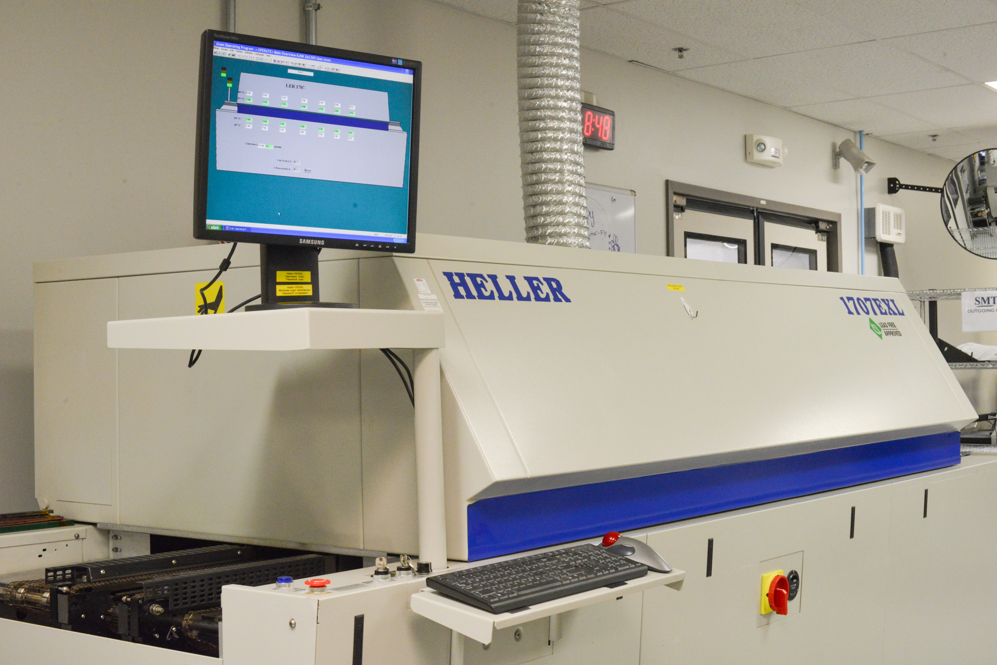
Despite an abundance of literature about oven reflow soldering, PICA has found that setting up a reflow profile remains a challenge to many. The following post is intended to provide process engineers with hands-on recommendations.
Reflow processes are generally defined by their heat application methods. Common examples include convection, infra-red (IR), conduction and vapor phase. Convection heating has become the dominant form of reflow primarily due to its heat application consistency, compatibility with Solder Paste technology and its high volume capability.
The principal process elements include:
- The panels to be assembled and their components.
- A conveyorized oven – usually consisting of 8 to 12 independent heating zones.
- A controller to monitor and control the conveyor’s speed and the temperature of each oven zone.
- The solder paste selected to support the product and its application. It consists of small balls of solder, bound together by a liquid composition (Flux), to allow proper deposition onto the board and support heat transfer and surface cleaning. Remember to always determine the solder paste manufacturer’s recommended profile.
- The customized transport fixturing to carry the board through the conveyorized ovens.
- A thermo couple to be attached to the boards to monitor the temperatures through the full length of the oven. The highest thermal mass locations on the board and the different locations on the fixturing both need to be monitored.
- A microscope with a power of at least 30X to inspect the solder quality.
Procedures to develop the reflow profile:
1. Run a panel with an attached thermal couple to obtain the product profile (an engineer’s educated guess is the best way to set the initial machine settings).
2. Repeat the above process until the profile complies with the manufacturer’s recommendation.
3. Apply solder paste to your first panel. Place components and process through the oven using the correct profile.
4. Inspect finished assemblies immediately out of the oven. Do not clean or remove from the panel or rework the boards before examining them.
5. Examine the boards; create a map identifying where the issues are located.
Interpreting the inspection results:
To make appropriate adjustments, the inspection results must be related to the phases of the reflow profile. Reflow profile phases include four zones:
- Ramp up
- Activation (of the Flux)
- Punch over (solder paste reflow)
- Cool down
Curious how your PCB designs are assembled with precision? Reflow soldering is a critical part of modern surface mount assembly. Learn how it works and how to optimize for it.
Common defects and their probable causes:
Solder splatter or small solder balls: a problem with the activation zone. Not enough flux evaporated, causing the flux to explode in the punch over zone.
Presence of liquid flux: same as the above.
Complete absence of flux or flux residue: A problem with the activation zone caused the flux to evaporate. No solder balls will be present. (To reduce pad oxidation, some leftover flux residue is necessary.)
Component displacement (e.g. rotated, tombstoned, edge flipped): Likely a pad design issue or possibly a placement issue. Pad size, grab factor pick & place positioning, solder deposits on pads, stencil design, etc. can also contribute to part displacement. A rotated component is often a programming issue or a component loaded incorrectly.
Solder wetting (solder filets are feathered to the board and components) or solder does not ball up: Solder not wetting properly is usually an activation zone issue. If the flux is fully evaporated prior to the assemblies entering the punch over zone, the solder balls and board pads may have oxidized or become contaminated with flux residue, preventing wetting. Time above liquidus (TAL) may also be the reason there’s not enough time to wet.
Grainy or “solder graping” conditions (resembles clusters of grape that adhere to each other): Grainy or solder graping can be an activation zone issue, in which oxidation or flux residue contamination causes the solder balls to melt together. It can also be a punch over zone issue caused by the solder not reaching the needed level of temperature or time above liquidus being too short.
Voids in solder: generally caused by flux explosion during the punch over zone. This is due to the activation zone not evaporating enough flux.
Solder transfer (solder which has migrated to a component or the PCB, leaving insufficient solder on the other): Too many possibilities exist for this condition.
Insufficient or excessive solder: this is a stencil issue not related to the oven.
